555 Timer Internal Schematic : 555 Timer - A Complete Basic Guide | Todays Circuits ... / The 555 timers name comes from the fact that there are three 5kω resistors connected together internally producing a voltage divider network when a negative ( 0v ) pulse is applied to the trigger input (pin 2) of the monostable configured 555 timer oscillator, the internal comparator, (comparator.
555 Timer Internal Schematic : 555 Timer - A Complete Basic Guide | Todays Circuits ... / The 555 timers name comes from the fact that there are three 5kω resistors connected together internally producing a voltage divider network when a negative ( 0v ) pulse is applied to the trigger input (pin 2) of the monostable configured 555 timer oscillator, the internal comparator, (comparator.. The schematic can be simplified somewhat to a block diagram making the operation of the circuit slightly easier to understand. The circuit latches in either the q state or its refer block diagram of 555 timer ic given above: Well here are a couple of schematics from the national semiconductor datasheet to help explain it. 555 internal schematic of bipolar version. Finally, power up your circuit by connecting the battery to.
Now a days it is manufactured by many companies in bipolar and in low power cmos. This integrated circuit can be used in a variety of ways from which the basic one is to produce accurate and stable delays in electronic circuits. • to understand how the capacitor is used in the 555 timer oscillator circuit, you must understand the basic charge and discharge cycles of the capacitor. 555 timer ic internal schematic. Look at the circuit diagram.
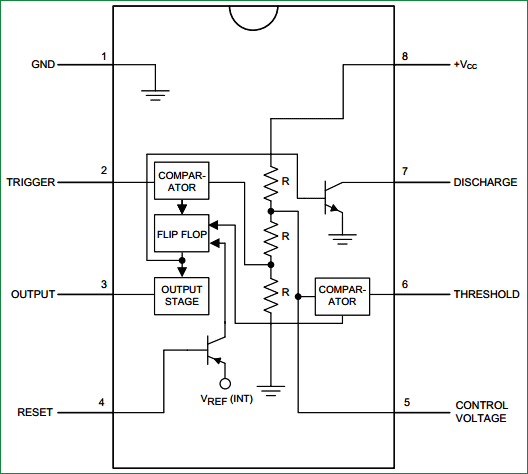
Panic Alarm Button Circuit using 555 Timer IC - ArRoboticsBlog from circuitdigest.com We can see that it us made up of 21 transistors, 4 diodes, and 15 resistors. The ne555, sa555, and se555 monolithic timing circuits are highly stable controllers capable of producing accurate time delays or oscillation. The timer will start when the wire is inserted into the protoboard between these two points, and ignore further contacts. This 0v pulse being below the 1/3rd level of the dc. Derivatives provide two (556) or four (558) timing circuits in one package. How it works, internal schematic and block diagram. The standard timer action of the ic 555 is initiated by introducing a 0 v trigger pulse at pin 2. It can be used as an oscillator, led flasher, tone if you see the internal block diagram of 555 timer ic then it consists of the following parts.
The 555 timer ic is an integrated circuit (chip) used in a variety of timer, delay, pulse generation, and oscillator applications.
(1) for all available packages, see the orderable addendum at the end of the datasheet. Well here are a couple of schematics from the national semiconductor datasheet to help explain it. It is a affordable, stable and user friendly ic in application such. This integrated circuit can be used in a variety of ways from which the basic one is to produce accurate and stable delays in electronic circuits. Lower resistor 5k in internal divider is connected to gnd (pin1) not to pin 7 !!!! The ne555, sa555, and se555 monolithic timing circuits are highly stable controllers capable of producing accurate time delays or oscillation. In the monostable mode, the timer generates a single pulse. 555 timer is an industrial standard ic existing from early days of ic. The 555 timer ic is an integral part of electronics projects. Here's the internal schematics of 555 timer which consists of 25 transistors, 2 diodes and 15 resistors. Due to its relative simplicity, ease of use and low cost it has been used in literally thousands of applications. The 555 timer ic is a very popular timer ic and it is widely used in many timing related applications. The 555 timer is a simple integrated circuit that can be used to make many different electronic circuits.
It can be used as an oscillator, led flasher, tone if you see the internal block diagram of 555 timer ic then it consists of the following parts. Well here are a couple of schematics from the national semiconductor datasheet to help explain it. Here's the internal schematics of 555 timer which consists of 25 transistors, 2 diodes and 15 resistors. Due to its relative simplicity, ease of use and low cost it has been used in literally thousands of applications. Get the detailed information about modes of 555 timer ic and.
Free Circuit Diagrams: Timer 555 Schematic from 3.bp.blogspot.com There are a lot of applications of this ic, mostly used as vibrators like, astable multivibrator, monostable multivibrator, and bistable multivibrator. It is a affordable, stable and user friendly ic in application such. The 555 timer is a simple integrated circuit that can be used to make many different electronic circuits. The 555 timer ic is an integral part of electronics projects. The 555 timer was introduced over 40 years ago. In the schematic above, notice that the threshold pin and. The 555 can be used with a supply voltage (vs) in the range 4.5 to 15v (18v absolute maximum). In astable mode, the 555 timer puts out a continuous stream of rectangular pulses having a specified frequency.
The 555 timer can operate in three different modes:
The circuit latches in either the q state or its refer block diagram of 555 timer ic given above: Today we're pleased to declare that we have. Look at the circuit diagram. We can see that it us made up of 21 transistors, 4 diodes, and 15 resistors. In the schematic above, notice that the threshold pin and. The first simply uses a normal 2n3904 garden variety transistor, and this works well when vcc < 9v. Let's take a closer look what's inside the 555 timer and explain how it works in each of the three modes. The 555 timer was introduced over 40 years ago. In this article, we will cover about 555 timers. In the monostable mode, the timer generates a single pulse. This integrated circuit can be used in a variety of ways from which the basic one is to produce accurate and stable delays in electronic circuits. Lm555 timer internal circuit block diagram. The internal resistors act as a voltage divider.
The schematic is designed in kicad. The ne555, sa555, and se555 monolithic timing circuits are highly stable controllers capable of producing accurate time delays or oscillation. Learn about the 555 timer and how it works in astable mode. The internal resistors act as a voltage divider. Today we're pleased to declare that we have.
Inverted 555 Timer CircuitElectronics Project Circuts from electroschematics.com File c555 internal circuitg wikimedia mons from 555 timer internal schematic , source:commons.wikimedia.org 1 minute 5 minute 10 thanks for visiting our site, articleabove (555 timer internal schematic unique) published by at. It can be used as an oscillator, led flasher, tone if you see the internal block diagram of 555 timer ic then it consists of the following parts. Its name is derived from three 5k ohm resistors ,connected in series used in it.the timer ic 555 timer was first introduced by signetics corporation in 1971 as se555/ne555. We can see that it us made up of 21 transistors, 4 diodes, and 15 resistors. 1 internal diagram of 555 timer. Resistor r1 is connected between vcc and the discharge pin (pin 7) and another resistor (r2) is connected between the discharge pin (pin 7). The 555 timer ic is an integral part of electronics projects. This circuit uses the 555 timer in an astable operating mode which generates a continuous output via pin 3 in the form of a square wave.
When vcc > 9v, the base to emitter junction starts to zener and.
Its name is derived from three 5k ohm resistors ,connected in series used in it.the timer ic 555 timer was first introduced by signetics corporation in 1971 as se555/ne555. The 555 timer ic is a very popular timer ic and it is widely used in many timing related applications. How it works, internal schematic and block diagram. There are a lot of applications of this ic, mostly used as vibrators like, astable multivibrator, monostable multivibrator, and bistable multivibrator. Look at the circuit diagram. 555 timer ic has basically three functional parts. 555 timer is an industrial standard ic existing from early days of ic. When vcc > 9v, the base to emitter junction starts to zener and. 1 internal diagram of 555 timer. The circuit latches in either the q state or its refer block diagram of 555 timer ic given above: The files are available for download at the end of the page. It's a simple source of oscillating current that can power blinking leds, generate tones, and lots of other useful applications. Finally, power up your circuit by connecting the battery to.
The image shown below represents the internal schematic of a standard ic 555 555 timer schematic. The files are available for download at the end of the page.


0 Komentar